Author Affiliations
Abstract
1 Institute of Micro-nano Photonics & Beam Steering, School of Science, Nanjing University of Science and Technology, Nanjing 210094, China
2 Centre for Disruptive Photonic Technologies, The Photonics Institute, School of Physical and Mathematical Sciences, Nanyang Technological University, Singapore 637371, Singapore
3 College of Physics and Electronic Information Science, Tianjin Normal University, Tianjin 300387, China
4 e-mail: jly@njust.edu.cn
5 e-mail: zexiang@ntu.edu.sg
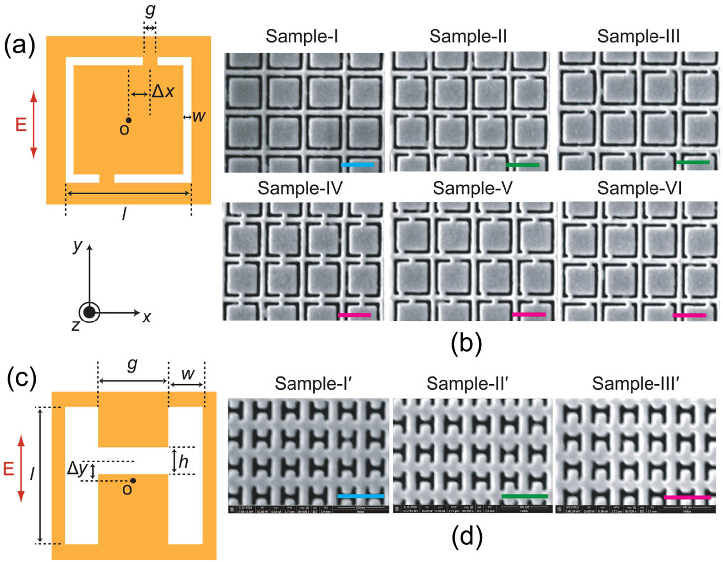
Understanding the mode’s origin in planar metamaterials is fundamental for related applications in nanophotonics and plasmonics. For complex planar metamaterials, conventional analysis that directly obtains the final charge/current distribution of a mode is usually difficult in helping to understand the mode’s origin. In this paper, we propose a mode evolution method (MEM) with a core analysis tool, i.e., plasmonic evolution maps (PEMs), to describe the mode evolution in several complementary planar metamaterials with designed plasmonic atoms/molecules. The PEMs could not only clearly explain a mode’s origin, but also reveal the role of a structure’s symmetry in the mode formation process. The MEM with PEMs can work as a simple, efficient, and universal approach for the mode analysis in different kinds of planar metamaterials.
Photonics Research
2021, 9(1): 01000073
Author Affiliations
Abstract
1 State Key Laboratory of Bioelectronics, School of Biological Science and Medical Engineering, Southeast University, Nanjing 210096, China
2 Department of Physics, School of Science, Nanjing University of Science and Technology, Nanjing 210094, China
Zero-mode waveguides have become important tools for the detection of single molecules. There are still, however, serious challenges because large molecules need to be packed into nano-holes. To circumvent this problem, we investigate and numerically simulate a novel planar sub-wavelength 3-dimension (3D) structure, which is named as near-field spot. It enables the detection of a single molecule in highly concentrated solutions. The near-field spot can produce evanescent waves at the dielectric/water interface, which exponentially decay as they travel away from the dielectric/water interface. These evanescent waves are keys for the detection of fluorescently tagged single molecules. A numerical simulation of the proposed device shows that the performance is comparable with a zero-mode waveguide. Additional degrees-of-freedom, however, can potentially supersede its performance.
Plasmonics single fluorescence molecule evanescent field zero-mode waveguide Photonic Sensors
2020, 10(4): 364
南京理工大学理学院信息物理与工程系, 江苏 南京 210094
采用离子源辅助电子束蒸发的方法,制备了以Si为基底,以TiO2为缓冲层的ZnO薄膜。通过进一步保温处理,在不同温度条件下进行退火处理得到了不同的样品薄膜,用于表面形貌分析和光散射特性实验研究。结果表明,退火温度对样品表面粗糙度、晶粒大小、分形维数等参数具有显著的影响,通过表面形貌分析有助于更好地理解薄膜晶粒生长机制和改进薄膜制备工艺;不同薄膜样品的反射光强度和偏振度对不同偏振光具有不同的角度响应特征,且与薄膜表面统计特性具有一定的关联性,薄膜的光散射特性研究对研究弱散射随机粗糙表面的退偏作用具有一定的参考价值。
薄膜 表面形貌 分形理论 光散射特性
Author Affiliations
Abstract
1 Department of Physics, Nanjing University of Science and Technology, Nanjing 210094, China
2 Nanoscale Technology and Engineering Laboratory, Department of Mechanical Engineering, Schulich School of Engineering, University of Calgary, Calgary, Alberta, T2N 2N4, Canada
3 Tanaka Metamaterials Laboratory, RIKEN, Saitama 351-0198, Japan
A concave two-dimensional (2D) photonic crystal waveguide (PCW) with corrugated surface is theoretically used as a focusing structure. To design this structure, a genetic algorithm is combined with the finite-difference time-domain method. For PCWs with different degrees of concaveness, the power reaches about 80% at different focusing points when the morphology of the concave surface is optimized. More importantly, the focusing location is easily controlled by changing the location of the detector placed in the output field.
光子晶体波导 遗传算法 聚焦效应 130.5296 Photonic crystal waveguides 130.3120 Integrated optics devices Chinese Optics Letters
2011, 9(1): 011301
1 南京理工大学理学院, 江苏 南京 210094
2 中国电子科技集团第二十八研究所莱斯大型电子系统工程有限公司, 江苏 南京 210007
利用二维光子晶体的自准直和定向耦合效应设计了一种由一个自准直区域、耦合区和两个周期性介质波导组成分束器, 利用平面波展开法从理论上研究了耦合区的色散关系, 计算得到了耦合长度, 同时使用时域有限差分方法模拟了电磁波在其中的传输特性, 得到了稳态的电场分布, 讨论了光波从自准直区域到光子晶体波导高效耦合的技术。结果表明:在相位匹配条件下, 从自准直区域传播到耦合区域的的电磁波可以有效的分束到两个周期性介质波导中, 同时能够弯曲任意角度, 而且透射率保持在90%以上。最后, 在设计的分束器基础上提出了一种增大点源和像点之间距离的方法。
集成光学 光子晶体分束器 同向耦合 自准直
采用了结构为(B′A′)N(A′B′)N (B′′A′′)N(A′′B′′)N的光子晶体异质结来设计一维全方向滤波器。利用传输矩阵法对该结构的透射性能进行了分析, 并结合遗传算法对该光子晶体异质内各组元厚度比和组元的周期数进行了优化, 最终得到一个相对较优的一维光子晶体滤波器。该滤波器具有较宽的滤波频带, 并且具有很好的方向选择特性, 是一种高精度的一维全方向光子晶体滤波器, 可广泛应用于滤波器、光开关等光通讯领域。
光子晶体 全方向滤波器 光子晶体异质结构 遗传算法
Author Affiliations
Abstract
School of Science, Nanjing University of Science and Technology, Nanjing 210094
The depolarization behavior of backscattered linearly polarized light from ZnO thin film was investigated experimentally. The results show that the characteristics are related to both the polarization orientation and wavelength of linearly polarized incident light. When the incident light is s-polarized, the depolarization behaviors are different for different wavelengths. When the incident light is p-polarized, the depolarization behaviors, on the contrary, are similar for different wavelengths. In addition, there is an optimal incident angle for depolarization of linearly polarized light with different wavelengths, which is equal to their effective Brewster angles, respectively.
退偏振 线偏振光 ZnO薄膜 有效布鲁斯特角 290.5880 Scattering, rough surfaces 260.5430 Polarization 240.0240 Optics at surfaces 290.0290 Scattering Chinese Optics Letters
2007, 5(12): 720


